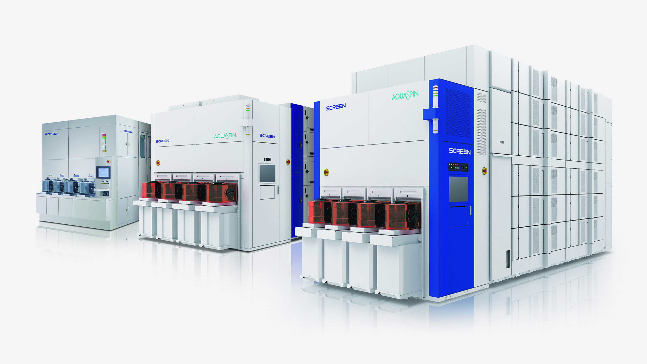
Headquartered in Kyoto, Screen Semiconductor Solutions Co. Ltd., which is celebrating over 80 years in business this year, holds the biggest global market share in semiconductor wafer cleaning systems, its core product. In a recent interview with The Japan Times, Representative Director and President Akihiko Okamoto and Cleaning Elemental Technology Development Department Head Hiroaki Takahashi spoke about the strengths of their wafer cleaning systems and their commitment to sustainability.
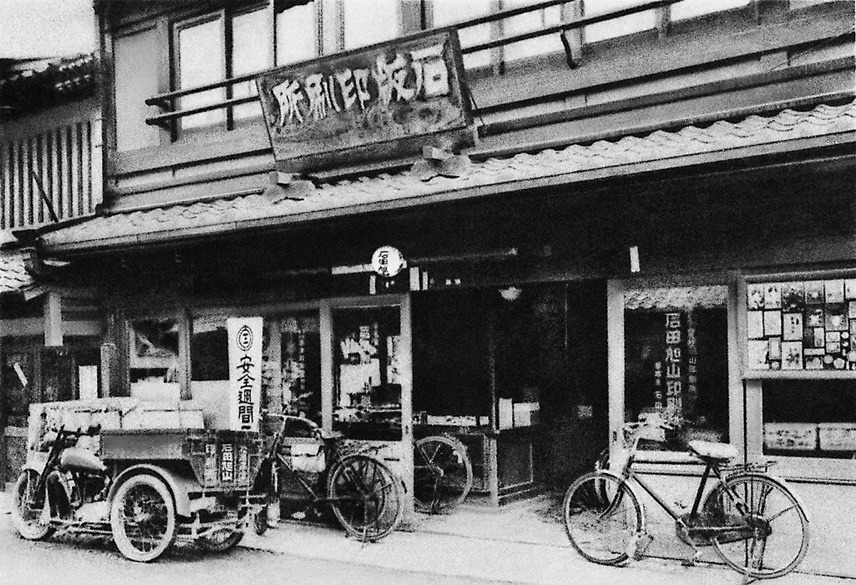
The company is part of Screen Holdings, which was formerly a printing company established in Japan in 1868. The Screen Group possesses three core technologies: surface processing, direct imaging and image processing. Each contains its component technologies that have been applied to the semiconductor, printing, display, printed circuit board and other markets.
Ensuring cleanliness
Among the core technologies, Screen specializes in surface processing, which is mainly used in equipment for cleaning semiconductors.
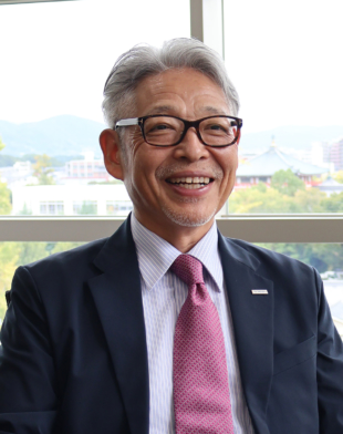
“In semiconductor manufacturing, cleaning the surface of semiconductor wafers is required at the completion of each process. If this cleaning is inadequate or insufficient, microscopic dust and dirt can interfere with the next process and affect the quality of the product, resulting in a lower yield rate,” Okamoto explained.
Screen’s ultra-clean, fluid control and drying technologies support the surface treatment process.
“We are particularly focusing on our ultra-clean technology. The cleaning process varies widely and in complexity, depending on the type of semiconductor device and the process used to make it. This technology is designed to satisfy all needs while ensuring that all impurities are removed without fail,” Takahashi said.
In addressing the complexity of the process, Takahashi explained that several chemicals are used separately in some cases and mixed in others, while temperature also varies according to each case.
“For example, when it is necessary to use multiple chemicals separately at high temperature, we need to ensure that the chemicals in their liquid form won’t mix together. But the real challenge lies in how to prevent the chemicals that evaporate at high temperature from reacting with each other or coming into contact with other chemical solutions inside the equipment, creating unwanted results. Another issue is how to maintain the route for supplying the chemicals clean,” he said.
Screen customizes and optimizes its wafer cleaning systems to cater to each unique case, making sure that any potential problems are addressed. Their wafer cleaning systems can be categorized into two basic types, one for logic semiconductors — the smallest and most sophisticated ones made for high-level computing mainly in smartphones and computers — and the other for legacy chips that are commonly found in automobiles, appliances and consumer electronics.
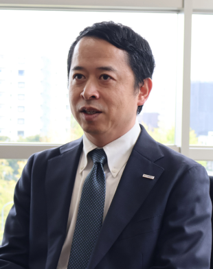
“But even within these two categories, there is great diversity in the processes for manufacturing chips, and the levels and functions required of wafer cleaning systems are different as well,” Takahashi said.
Support from R&D
The Screen Research and Development Department comprises four areas: basic research, component technology development, product development and equipment evaluation, with each group communicating closely with the corresponding team at each customer.
The company collaborates on high-level, time-consuming basic research with schools such as Shiga University and Mie University, as well as national research institutes. The achievements of the basic research are used in the development of element technologies where the company engages in joint R&D with front-line consortiums, such as the Interuniversity Microelectronics Centre (IMEC) in Belgium and the Alternative Energies and Atomic Energy Commission collaboration with the Electronics and Information Technology Laboratory in France.
In the areas of product development and equipment evaluation, new technologies and equipment are developed and evaluated through collaboration mainly with other companies.
“It is important that we work with other companies in the long and complex semiconductor supply chain, including our suppliers, such as manufacturers of valves, filters and chemicals,” Takahashi said. New technologies and equipment are then further assessed at customer production sites before they are finally installed on the production lines at the sites.
Takahashi said the company employs science-based methods in all steps in its research and development process, even where the intuition and experience of engineers have conventionally been depended on. “We want to pursue science-backed optimal solutions to further improve the sophistication of our technology development,” he said.
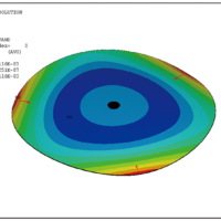
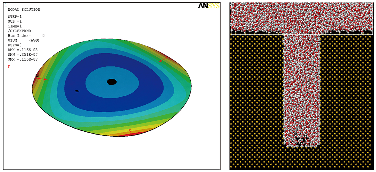
One example of such efforts is the use of computer simulation. “Take computer fluid dynamics as an example. It’s a technology used to find the best way to cover wafers with liquid by simulating how liquid will spread when it is poured onto the horizontally rotating surfaces of wafers in the wafer cleaning systems,” Takahashi said.
Another example is related to the drying technology used in the equipment. “Just like a woolen sweater shrinks when it is washed without adequate care, the structure of semiconductors is also affected by drying. Instead of making assumptions about how exactly this nanometer structure is influenced, we are trying to visualize the impact based on calculation and modeling as part of our joint research with a Japanese university at the moment,” Takahashi said.
Pursuing sustainability
It is not just the area of cleaning technology that requires joint R&D with stakeholders. Basic conservation is an issue as well. “Throughout the long process of making chips, vast amounts of electricity and pure water are required. It is a big challenge for all in the supply chain to reduce their consumption,” Okamoto said.
During the past several years since returning from Singapore in 2021 after heading Screen’s local branch for 5 1/2 years and becoming president of Screen Semiconductor Solutions in April, Okamoto has felt rising interest in sustainability emerge among the company’s customers. Takahashi said the trend cannot be ignored.
“We have been conducting regular technical meetings dedicated to issues of sustainability with some of our customers since about three years ago. Requests from customers related to sustainability have become increasingly specific and concrete,” Takahashi said.
Okamoto said that he considers this trend an opportunity for the company to enhance its value and that the company will continue to focus on its efforts to increase environmental sustainability in the semiconductor industry.
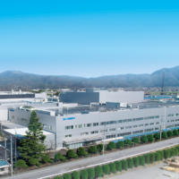
The company’s plant in Hikone, Shiga Prefecture, uses electricity from renewable energy sources and facilities that consume less electricity than conventional ones. For the products the company manufactures, there is a set of evaluation standards established for the purpose of promoting products that are environmentally friendly both in the manufacturing process and when used. Products that meet the standards are certified as “green products.” Efforts to make products greener include curbing their electricity consumption and carbon emissions, reducing the amounts of chemicals used, or looking for less harmful materials to use. “This way, we ensure that all our newly released products are labeled as green products,” Takahashi said.
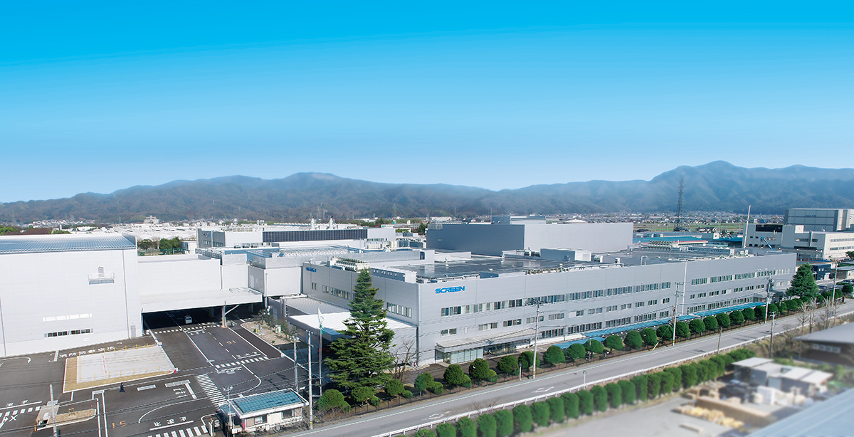
Okamoto revealed that there are also demands to improve the efficiency of electricity and water use for its existing equipment.
“Our wafer cleaning systems use heated ultrapure water to clean the insides of itself. This water had conventionally been single use, but we developed a system that allows the water to be circulated and reused. Our customers are very satisfied with it, and we are aiming to deploy it worldwide,” he said.
Okamoto pointed out that progress is being made to improve the cleaning process for semiconductors because it requires a significant amount of pure water.
“We started using a water management application to track and visualize how much water we are using and to analyze how we can reduce it. Now that we have gathered enough figures by using this application, we are starting to work on reducing our water usage,” he said.
However, the amount was not the only problem. The company’s research on its carbon emissions begun two years ago has revealed that using ultrapure water results in the greatest amount of carbon dioxide emissions among all other equipment at the company.
Takahashi explained this was because the conventional water heating unit was working even when water was not needed. This was to prevent the water temperature from dropping and the water flow inside the cleaning unit from becoming inconsistent.
A new water heater the company developed can heat it and supply it to the equipment only when needed, based on the concept of “smart use.”
“Thanks to this new system, we have managed to reduce not only the amount of ultrapure water, but also the electricity consumption related to the water by 85%, resulting in lower emissions,” Takahashi said.
Okamoto noted that each country has its own priorities when it comes to sustainability. The highest priority, whether it be water, electricity or something else, depends on various factors, including the country’s environmental, social, economic and political situations. Screen is committed to customizing its efforts to customers in each country.
On the other hand, he emphasized that the carbon emissions issue needs to be addressed collectively by the entire semiconductor supply chain. As a member of the Semiconductor Climate Consortium (SCC) within Semiconductor Equipment and Materials International, a global association of more than 3,000 members from the industry, the company aims to take the initiative in conducting advanced carbon emission analysis of the supply chain and sharing effective practices with other members of the SCC. One of the projects the company engages in within the SCC involves the use of Zeroboard, a cloud-based tool that enables the calculation and visualization of greenhouse gas data.
“We use it to analyze where specifically in our supply chain environmental stress is significant so that we can better understand how to effectively minimize it,” Okamoto said.
He added that the company is also collaborating with IMEC and other stakeholders both in Japan and abroad, which has expanded the technical boundaries of the supply chain in environmental sustainability. “However, as a result, we are faced with mounting costs,” he said, stressing that in addition to a collective effort in covering the costs, it is important to call for support from the government to not hamper the industry’s progress in becoming greener.
Global benefit of semiconductors
More than 80% of Screen Semiconductor Solutions’ customers are companies in countries and regions such as Taiwan, South Korea, the United States, Europe and China. Takahashi said the company aims to give its customers the value of time wherever they are.
“To shorten the time at all stages of manufacturing and operating our equipment including the time for product development, installation, downtime and recovery, enabling the world to continuously receive the benefit of the most up-to-date semiconductors, we need to improve the intelligence of our equipment,” he said.
Beyond that is the application of technologies to develop a “digital twin,” a virtual model created and constantly updated in real time based on data gathered in the real world, that would allow them to create products based on accurate analysis of how exactly they should be designed, backed by science and theory, naturally resulting in shorter delivery times and higher reliability, he said.
But changes in manufacturing also mean changes in what is expected of engineers.
“It is increasingly important for engineers to have the ability to come up with ideas about what society needs and what kind of technology can be useful, and the communication skills to engage our customers and other stakeholders to realize the ideas,” Takahashi said.
Okamoto said that he encourages all employees of the company, not just engineers, to feel confident their work has a social value in both direct and indirect ways.
“Our equipment and our environmental efforts directly contribute to society, while semiconductors, which cannot be produced without our cleaning technology, contribute to solving social issues around the world,” he said.
This article is sponsored by Screen Semiconductor Solutions Co. Ltd.


