Diamonds are commonly referred to as the hardest naturally occurring substance known to humankind. The chemical composition is extremely simple — carbon atoms, and nothing more. But the arrangement of those atoms in a particular lattice structure is what gives the substance its unique properties.
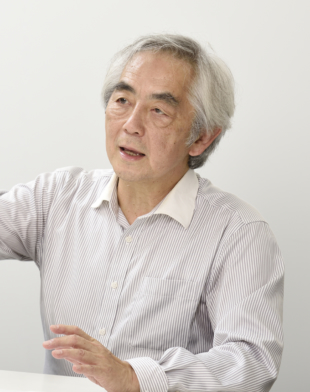
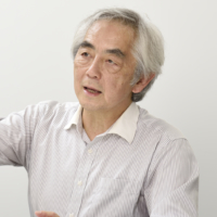
To date, silicon has been the primary raw material for making semiconductors owing to its stable structure. However, as professor Hiroshi Kawarada of the School of Fundamental Science and Engineering at Waseda University points out, diamond — whether natural or manmade — has the same structure as silicon but with superior electric properties.
“Diamond is an even better insulator,” he said. “We can control thermal conductivity much better, making it ideal for semiconducting and superconducting applications,” he said.
Easy to make
Diamond, along with carbon nanotubes, can be used to develop ultra-high-speed, high-power transistors, supersensitive nano biosensors and superconducting devices. As Kawarada explains it, this is because these materials have strong bonds and can withstand high electric fields and temperatures, while also having a high affinity for biomolecules and other substances.
“Heat dissipation in transistors is very, very important,” Kawarada said. “Heat is generated when conducting electricity, and getting good thermal conductivity is difficult, so this makes diamond a very good material to use.”
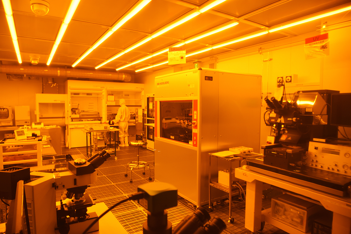
This characteristic, he argues, makes semiconductors with diamond-based circuits very useful for electric vehicle applications, where their ability to also tolerate high voltages gives them an added advantage. Moreover, the heat dissipation performance also would make such semiconductors useful for graphics processing units. GPUs, he pointed out, are frequently used in the training of artificial intelligence models. They generate quite a lot of heat with the work they have to do, and so a diamond-based semiconductor could help to keep the heat under control.
Thanks to their thermal conductivity and insulating performance, diamond-based semiconductors can also have applications in the fields of personal computers and smartphones, he noted.
With respect to smartphones in particular, it is not just in the phones themselves but also in base stations through which signals are transmitted. Base stations need to withstand a wide range of environmental conditions, from hot temperatures in summer to cold in winter. Ideally, he explained, base stations should be installed in an air-conditioned space to keep them at a constant temperature, but this may be overlooked by some carriers due to the additional expense. Moreover, they also want base stations to be as small as possible. Given the heat generated within such small spaces and fluctuating temperatures in the external environment, diamond-based semiconductors again have an edge, Kawarada emphasized.
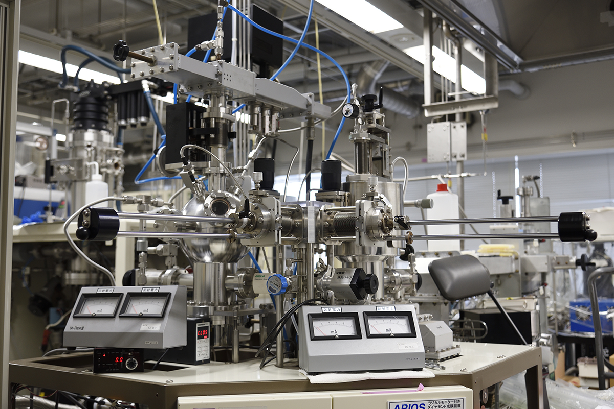
Tangentially, diamond also has an environmental benefit in terms of how it is made, Kawarada added. Diamond can be made by taking two greenhouse gases out of the atmosphere, methane and carbon dioxide. When the manufacturing process is complete, the result is diamond and the waste product is simple water. Compared with silicon, diamond is quite simple to make, he said. It is very good for semiconducting once it is combined with metals, and the result can be used to make semiconductors. The ease of this process has an educational benefit, he added, in that “it makes it very easy to teach to our advanced undergraduates how to make a transistor. It is very good to help our students learn how semiconducting devices work.”
Into the future
These materials and the notion of diamond-based semiconductors are being further explored through a start-up venture Kawarada co-founded at Waseda in August 2022 — Power Diamond Systems. This start-up, which also maintains a research and development center in Kitakyushu, is a research-driven operation that aims to “realize the social implementation of diamond semiconductor power and high-frequency devices.”
“It is true that there are two dozen other diamond-substrate companies like ours around the world, including at least two or three others here in Japan. One thing that I believe sets us apart is that we are working to make transistors that are based on substrates, and these transistors can then be used in other applications,” he said.
PDS develops these prototype devices, but does not sell them by itself, he hastened to add, saying, “To actually develop and produce commercial devices ourselves would take a lot more time, and require more resources.” PDS is focused on doing the kind of exploratory research and development work that a major company might want to do, but perhaps does not have the time or expert staff. The most important potential application for the transistors that PDS is working on is power electronics, he explained.
Traditionally, silicon carbide has been used for high-voltage power devices, such as the inverters that control electric vehicle motors. What is needed, he said, are transistors that can carry high voltages and are very efficient, and PDS believes that diamond will take power devices to the next level.
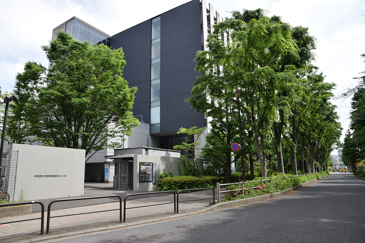
This article is sponsored by Waseda University.
Waseda University

Address: 1-104 Totsukamachi, Shinjuku-ku, Tokyo 169-8050
Phone: +81-3-3202-5454
E-mail: [email protected]
URL: https://www.waseda.jp/top/en/


