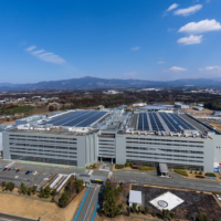
The Sony Semiconductor Solutions Group holds the largest share in the rapidly growing imaging sensor market in terms of revenue. It focuses on advanced technologies and excellent quality, aiming to accelerate the further expansion of social implementation through technological advancement.
Image sensors: A growing market
Image sensors are semiconductors that are also called “electronic eyes.” Most of the current applications are for smartphone cameras; however, image sensors have also become essential for autonomous driving technology, factory automation, artificial intelligence integration and edge computing. Between fiscal years 2023 and 2030, the image sensor market is expected to have a compound annual growth rate of 9%.
An independent subsidiary of the Sony Group since 2016, Sony Semiconductor Solutions has a long history in image sensor development. In the 1970s, the company succeeded in mass producing the world’s first charge-coupled device image sensors. Although having established a dominant market position with CCDs, the company made the decision in 2004 to halt investment in CCDs and shift its development resources to something known as a complementary metal-oxide-semiconductor image sensor. CMOS sensors at that time had issues with image quality compared with CCDs; however, forecasting demand for significantly improved image quality for video recording and the use of mobile devices in the near future, the company decided to turn its full attention to developing a high-performance version of CMOS.

In the more than 20 years since, Sony Semiconductor Solutions has launched a number of world-first technologies that have led the company’s CMOS image sensor to significantly exceed CCD performance, producing new trends and markets with its excellent image quality as well as unique features to function as the eyes of various electronics. According to its research, in fiscal 2023, it achieved an astonishing 53% market share in value, well ahead of its competitors.

“I feel that this number reflects the market’s recognition of our high-performance products with exceptional and consistent quality that satisfy customer needs,” said Terushi Shimizu, the company’s representative director, president and CEO.
‘Creation technology’
Sony Group has outlined the company’s strategic direction as “Creation Shift,” which means that Sony is shifting its focus towards creation side in each business layers to create kando (emotion) together with creators. The company’s image sensors are essential creation technology for the growth of the group as it strives to achieve this forward-looking shift. Image sensors are mounted on mirrorless interchangeable-lens cameras and digital cinema cameras used in film production, contributing greatly to creation efforts. Furthermore, cameras installed in smartphones are now indispensable tools used every day to make every user a creator.
“Smartphone manufacturers consider cameras to be important elements in differentiating their products from others and strive to develop high-performance camera systems, especially for high-end models. Sensor performance is a key factor for achieving high-quality still images and video taken under a wide variety of conditions, and it significantly influences total camera performance,” Shimizu said.

In addition to a larger sensor format that increases the light-receiving area, Sony Semiconductor Solutions is working on improving the key characteristics that determine image quality and continues to make steady progress on the long-term development road map.
Given the unstoppable growth of the image sensor market, the company has steadily increased capital investment to enhance production capacity, committing a total of ¥930 billion over the three years from fiscal 2021 to 2023. The company also has funded the expansion of its Nagasaki Technology Center’s new Fab 5 and continues improving the facilities, while recently acquiring land in Kumamoto Prefecture next to its existing Technology Center to build a new fab primarily for image sensors. Furthermore, Sony Semiconductor Solutions has invested in Japan Advanced Semiconductor Manufacturing, which was established as a subsidiary of Taiwan Semiconductor Manufacturing Co., the world’s largest semiconductor foundry, also in Kumamoto. Through this strategic investment in JASM, Sony Semiconductor Solutions aims to reinforce its partnership with TSMC, while aiming for stable procurement of logic wafers used for the company’s stacked CMOS image sensors.
“With globally expanding semiconductor demand, JASM is expected to contribute to the stable supply of logic wafers not only for Sony Semiconductor Solutions, but for the entire semiconductor industry as well. For the Japanese semiconductor industry, the establishment of JASM will stimulate the business initiatives of corporations involved in semiconductor manufacturing, leading to a revitalization of the overall industry,” Shimizu said.

The company, which has broadened its customer base and achieved a high market share, is expanding its sensing capabilities and services for utilizing image information by incorporating various technologies into its image sensors. These chips are already being implemented in society for wide range of applications in various sectors, including automotive, machinery, industrial and the Internet of Things.
“Sony Semiconductor Solutions has provided sensors not only for smartphones and digital cameras, but also for a wide range of applications and has accumulated a variety of technologies over many years. Such comprehensive sensing technology capabilities in image sensor technology are one of the strengths that differentiates us from our competitors, and we aim to strengthen our business by further diversifying our products and customers,” Shimizu said.
With increased attention gathering around advanced driver-assistance systems and autonomous vehicles, the company has increased engagement with global original equipment manufacturers and other partners. According to Sony’s research, this will allow the company to grow its share of automotive image sensors in value from 32% in fiscal 2023 to a projected 43% in fiscal 2026.

As the “eyes of vehicles,” image sensors require high-precision object recognition capability even under unfavorable conditions such as darkness, backlight or bad weather. The company aims to promote safe, secure and comfortable transportation spaces by enabling both internal and 360-degree external monitoring around vehicles via sensing technologies that exceed human eyesight.
Industrial markets are another focus area as the company faces a new challenge in the solutions business, which is centered on its core image sensor technologies. In this area, the company is forging ahead of others to address the heavier cloud and environmental loads caused by the increase of IoT devices. The demand for vision sensing via cameras has been climbing significantly in the IoT era. However, given the vast amount of data processed via cloud computing, a large number of issues ranging from increased network loads and power consumption to privacy risks, have also become apparent.
To address these issues, Sony Semiconductor Solutions launched its edge AI sensing platform Aitrios, a one-stop environment for various solution builders to efficiently and reliably develop products that rely on image sensors. Aitrios is making great progress, and the results re already becoming visible in the retail, logistics and factory markets.
Realizing a ‘sensing society’
All of the company’s technological efforts are being accelerated by its commitment to contribute to building a sensing society.
“We strive to improve technology and corporate value to open the door to an efficient and affluent future. To do so, it is essential for us to increase our presence in society, gain the understanding and cooperation of a wide range of stakeholders, including partner companies and local communities, and to work together to create social value. We hope to use our sensing technology to create new economic value by linking it to a more affluent society and to convenience in daily life,” Shimizu said.

The greatest challenge for a regionally rooted semiconductor business is the substantial water and electricity required for manufacturing. Based on the Road to Zero, the Sony Group’s long-term environmental plan, Sony Semiconductor Solutions has enhanced its approaches to reducing greenhouse gas emissions at each office and plant as its responsibility for the environment.
These approaches include the implementation of cutting-edge energy-saving technologies, the promotion of energy circulation and the adoption of renewable energy sources by combining solar panels with the purchase of Renewable Energy Certificates. As an integral part of its water resource preservation, the company also collects and reuses the majority of its wastewater.
Shimizu added: “Since its foundation, Sony has kept true to its spirit of challenging itself to achieve what others have not. Such activities motivate employees to explore new fields, resulting in the development of remarkable technologies. In addition, our company continues to identify the kind of added value that customers and partner companies around the world expect through close communication with them. Our drive to learn from the world, enthusiasm to create a positive future with our technology, and creativity that defies conventional wisdom have become the motivating power behind Sony Semiconductor Solutions’ development of image sensors that satisfy customers. To realize a safe, secure and affluent sensing society, we continue seeking improvements that have a significant impact.”
This article is sponsored by Sony Semiconductor Solutions Corp. Visit https://www.sony-semicon.com/en/index.html for more information.


