In October 2023, 123 years after Toppan Printing was founded in Tokyo in 1900, the group was reorganized into a holding company structure with Toppan Inc. as the core operating company. Based on a wide variety of technologies accumulated through its printing business, Toppan has established information and communication, living and industry, and electronics as its three major business segments. The electronics business achieved ¥266.5 billion in net sales for fiscal 2023, accounting for 16% of its total consolidated sales.
“You may wonder why a printing company is now involved in the electronics business; but we’ve actually been expanding our interests in electronics through our proprietary technology for more than 60 years since we started applying our photographic engraving technology in the manufacture of filters for sugar production,” said Kazunori Katsumura, an executive officer and deputy head of the electronics division. Regarding the semiconductor business, Toppan has advanced technological capabilities for the high-end flip chip ball grid array (FC-BGA) substrates, next-generation semiconductor packages and photomasks for semiconductors, and has been involved as a substrate manufacturer in the TSMC 3DFabric Alliance. These business activities have been highly regarded in markets around the globe.

Substrates for blazing data speeds
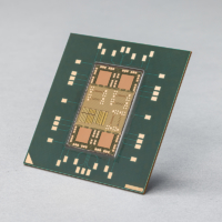
Toppan is proud of its more than 20-year history in the mass production of FC-BGA substrates. Initially, its focus was on FC-BGA substrates used for game consoles; however, Toppan reached a turning point in 2007.
Akihiko Furuya, Toppan’s executive officer and head of semiconductor business in the electronics division, proudly said: “With the appearance of iPhones, data communication quantity rose dramatically to 10 times that of previous levels. Based on the assumption that the quantity of data communication at mobile phone base stations would also increase, Toppan shifted its core semiconductor substrates to those used for network devices at base stations, and then expanded to semiconductor substrates for data centers. We continued seeking the most ideal semiconductor substrates that would correspond to high-speed transmissions, and we are quite confident in the formation of high-speed transmission lines and the quality of the signals.”
While competitors have developed technologies for personal computers and other consumer products, Toppan focused on network switches, high-frequency devices and other industrial-use products to achieve superiority, which built confidence in its semiconductor substrate production. Large-scale substrates (98 millimeters × 95 mm and 90 mm × 90 mm) will be exhibited at Semicon Japan 2024.
Toppan has responded flexibly to technological requirements such as increased substrate sizes and layers, and high-speed transmissions focusing on the development of large and multilayered FC-BGA substrates targeting server processers, network devices, home-use game devices, central processing units and graphics processing units.

“We have specialized in technology that forms high-speed transmission lines corresponding to a rate of 224 gigabits per second per line with four-level pulse amplitude modulation, and have achieved high-volume production of FC-BGA substrates. Recently, artificial intelligence accelerators employ extremely high-speed GPUs, and switches connecting accelerators also require high-speed transmission capability. This is where our FC-BGA substrates, which are capable of high-speed transmission, exert real strength. We have also produced a high-volume of large, multilayered 100-mm-square 9-2-9 build-up substrates for the market,” Furuya added.

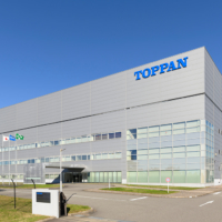
The Niigata Plant is producing high volumes of FC-BGA substrates, and the Phase 3 expansion production line is scheduled to start operation in 2026. To further strengthen productivity and support business continuity for the Niigata Plant, construction is ongoing at the Singapore Plant with plans to start operations at the end of 2026.
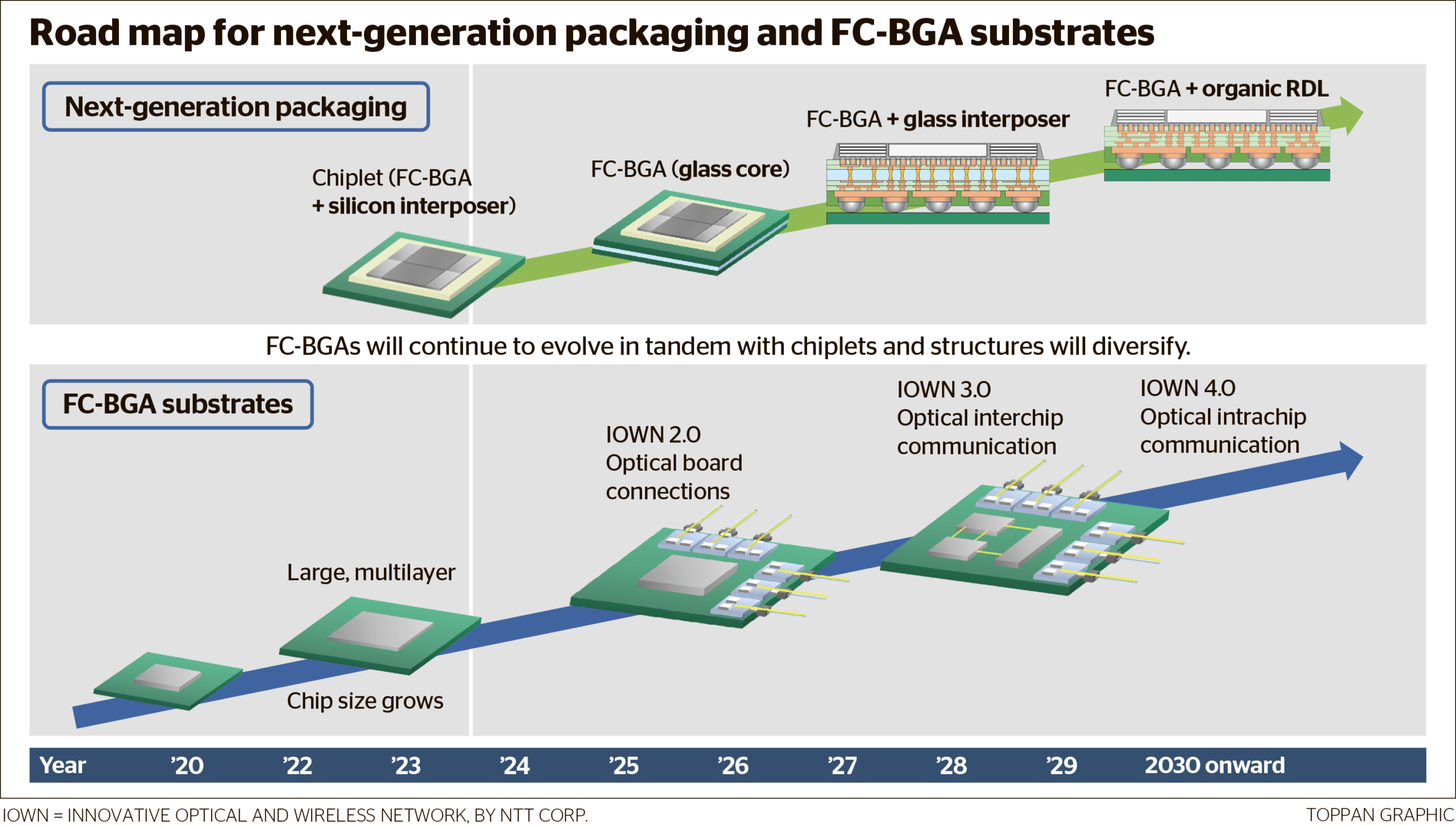
In the FC-BGA substrate business, Toppan is working on the development of substrates corresponding to photonics-electronics convergence technology represented by NTT’s Innovative Optical and Wireless Network 2.0, which requires further high-speed transmission.
“We are working jointly with a customer to develop FC-BGA substrates corresponding to copackaging which mounts photoelectric conversion elements onto the substrate, and we are about ready for market launch,” Furuya said.
This technology corresponds to ultra-high-speed switching at 102.4 terabits per second. Toppan is enhancing research and development considering optical transmission inside FC-BGA substrates (optical interconnections between chips) and intrachip optical interconnection as the next stage of optical connection between boards.
Primed for generative AI
Toppan promotes technological development not only for conventional FC-BGA substrates, but also for next-generation semiconductor packages for generative AI. According to Furuya: “Next-generation semiconductor packages will not eliminate FC-BGA substrates, but will develop a chiplet structure, which has multiple semiconductor chips mounted in an interposer installed onto an FC-BGA substrate. In response to this trend, Toppan is planning to enter the interposer market while maintaining its presence in the conventional FC-BGA substrate market.”
Toppan focuses on the development of high-productivity interposers for next-generation semiconductor substrates using glass and other organic materials. Different from silicon interposers that can be created only from circular wafers, glass and other organic materials will make it possible to manufacture interposers from rectangular panels. As a part of this technological development, Toppan established the Advanced Semiconductor Packaging Development Center in April.

“We have a wide variety of specialists on the development team with extensive experience in important areas, including design engineers for design and microfabrication processing in semiconductor front-end process, photomask engineers for microfabrication processing, and liquid crystal display color filter engineers for glass processing and transferring technology. The development of organic redistribution layer (RDL) interposers requires the ability to design the semiconductor front-end process, an area in which Toppan can exert its strength in semiconductor design services. Toppan has prepared research and development along with technological development structures by gathering knowledge from throughout the group.”
For generative AI, Toppan develops substrates for chiplet packaging combining FC-BGA and silicon interposers as it advances technological development of next-generation package substrates with glass cores, glass interposers and organic RDL interposers using glass carriers considering the potential for future popularization of chiplets. These technologies, which have attracted increasing attention, will be exhibited at Semicon Japan 2024.
Glass substrates

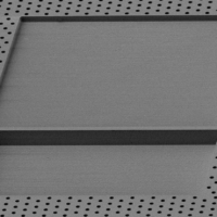
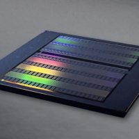
Toppan utilized glass processing technology that it has accumulated over the years to develop glass substrates having through glass vias (TGVs) with cavities of different depths for mounting in components. Toppan also succeeded in simultaneously processing TGVs and cavities. This can be applied to glass-core FC-BGA substrates and glass interposers. While there was concern about breakage in glass-core substrates caused by stress, Toppan was successful in preventing this problem. Toppan is exhibiting a sample at Semicon Japan 2024 that forms cavities and TGVs on a 510 mm × 515 mm glass panel without metallization.
RDLs by damascene processing
In addition to microfabrication technology nurtured in its FC-BGA business, Toppan utilizes a new damascene wiring formation developed from the semiconductor front-end process for chip-last type organic RDLs. After mounting an RDL (wiring layer) with glass carrier onto an FC-BGA substrate, the glass carrier is removed and chips are mounted. Toppan is exhibiting a sample at Semicon Japan 2024 that forms micro wiring (line/space = 2/2 micrometers) on a 510 mm × 515 mm glass panel with damascene processing method.
Coreless organic interposers

Toppan has developed a coreless organic interposer, the Toppan RDL Embedded Coreless Substrate, an example of innovative technology for packaging that increases the functionality of semiconductors. Interposers have three requirements to ensure the reliability of connection: low coefficient of thermal expansion (CTE) to approach the CTE of chips; fine pitch interconnections corresponding to the increase in input and output; and increased size corresponding to increases in the number of mounted chips. Coreless organic interposers capable of heterogeneous integration meet these requirements.
First, this new coreless organic interposer reduces CTE mismatches between chips and the FC-BGA substrate with a low-CTE material, adding structural rigidity to make it possible for the first time in the world to enable standalone electrical inspection without any carrier. And since these can then be delivered as a known-good-RDL, it improves mounting reliability and yield, making it possible to reduce loss due to chip disposal resulting from interposer defects.
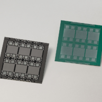
Second, this new interposer can be made in sizes exceeding 100-mm-square. Toppan is exhibiting a sample of four interposers as a unit at Semicon Japan 2024 that enables the largest increase in the manufacturing process currently possible in the industry (512 mm × 612 mm).

Toppan is developing new-generation semiconductor packages by combining these new technologies with FC-BGA at its Advanced Semiconductor Packaging Development Center, aiming to start mass production in fiscal 2028 at the Ishikawa Plant, which is now under construction. Toppan is also exerting unique technological capabilities in the next-generation semiconductor packaging business, and has undertaken the development of TSMC 2.5D packaging substrates. This is seen in its participation as a substrate manufacturer in the TSMC 3DFabric Alliance. Toppan is highly regarded for the quality and consistent supply of substrates it delivers for 2.5D packaging.
Photomasks gain top share
Toppan’s strength in the semiconductor business is not limited to FC-BGA substrates and next-generation semiconductor packaging. Katsumura noted: “Toppan has gained the top market share in the external sales market for photomasks, which are essential components in semiconductor manufacturing. Our products cover a wide range of processes, from the conventional to cutting-edge innovations, and sales of our photomasks have expanded to global markets.”
The development and manufacture of Toppan’s photomasks are handled by Toppan Group company Tekscend Photomask Corp. (rebranded from Toppan Photomask Co. Ltd. to Tekscend Photomask Corp. on Nov. 1). “Having eight manufacturing bases around the world, Toppan’s global reach in the photomask business is impressive. This coverage means that even when product demand is concentrated at one plant, Toppan has the backup structure to support manufacturing at other plants. We can leverage cooperation among our bases to effectively respond to short-term delivery,” Katsumura said.

Toppan develops different types of photomasks, including binary masks, phase-shift masks, and extreme ultraviolet photomasks, the top choice for next-generation photolithography. In February, Toppan signed an agreement with IBM for joint research and development of EUV photomasks, supporting microfabrication of semiconductors through the manufacture of cutting-edge photomasks. Toppan also plans to exhibit its EUV photomask at Semicon Japan 2024.
Katsumura speaks enthusiastically about Toppan’s participation in Semicon Japan 2024, “As the semiconductor business is attracting increasing attention both here in Japan and around the globe, we are pleased to have this opportunity to meet and speak with visitors in a wide range of industries at Semicon Japan 2024. I am looking forward to showcasing Toppan’s impressive strength in the semiconductor business to the world.”
This article is sponsored by Toppan Inc.


